 | –≠–ª–µ–∫—Ç—Ä–æ–Ω–Ω—ã–π –∫–æ–º–ø–æ–Ω–µ–Ω—Ç: THAT4301 | –°–∫–∞—á–∞—Ç—å:  PDF PDF  ZIP ZIP |
THAT Corporation; 45 Sumner Street; Milford, Massachusetts 01757-1656; USA
Tel: +1 (508) 478-9200; Fax: +1 (508) 478-0990; Web: www.thatcorp.com
T H A T
C o r p o r a t i o n
THAT An a log En gine
Æ
IC Dy nam ics Pro ces sor
THAT
4301, 4301A
FEA TURES
∑
High-Performance Volt age
Con trolled Am pli fier
∑
High-Performance RMS-Level
De tec tor
∑
Three Gen eral-Purpose Opamps
∑
Wide Dy namic Range: >115 dB
∑
Low THD: <0.03%
∑
Low Cost
∑
DIP & Sur face-Mount Pack ages
AP PLI CA TIONS
∑
Com pres sors
∑
Lim iters
∑
Gates
∑
Ex panders
∑
De-Essers
∑
Duckers
∑
Noise Re duc tion Sys tems
∑
Wide-Range Level Me ters
De scrip tion
THAT 4301 Dy nam ics Pro ces sor, dubbed
"THAT An a log En gine," com bines in a sin gle IC
all the ac tive cir cuitry needed to con struct a
wide range of dy nam ics pro ces sors. The 4301
in cludes a high-performance, ex po nen -
tially-controlled
VCA, a log-responding
RMS-level sen sor and three gen eral- pur pose
opamps.
The VCA pro vides two op pos ing-polarity, volt -
age-sensitive con trol ports. Dy namic range ex -
ceeds 115 dB, and THD is typ i cally 0.003% at 0
dB gain. In the 4301A, the VCA is se lected for
low THD at ex tremely high lev els. The RMS de -
tec tor pro vides ac cu rate rms-to-dc con ver sion
over an 80 dB dy namic range for sig nals with
crest fac tors up to 10. One opamp is ded i cated
as a cur rent-to-voltage con verter for the VCA,
while the other two may be used for the sig nal
path or con trol volt age pro cess ing.
The com bi na tion of ex po nen tial VCA gain con -
trol and log a rith mic de tec tor re sponse -- "deci -
bel-linear" re sponse -- sim pli fies the
math e mat ics of design ing the con trol paths of
dy nam ics pro ces sors. This makes it easy to de -
sign au dio com pres sors, lim it ers, gates, ex -
pand ers, de-essers, duckers, noise re duc tion
sys tems and the like. The high level of in te gra -
tion en sures ex cel lent tem per a ture track ing be -
tween the VCA and the de tec tor, while
min i miz ing the ex ter nal parts count.
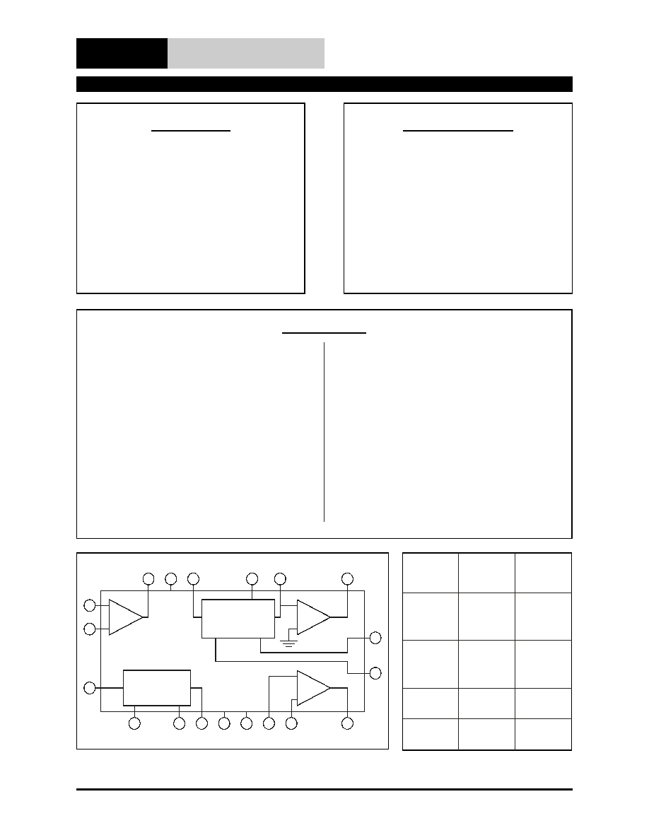
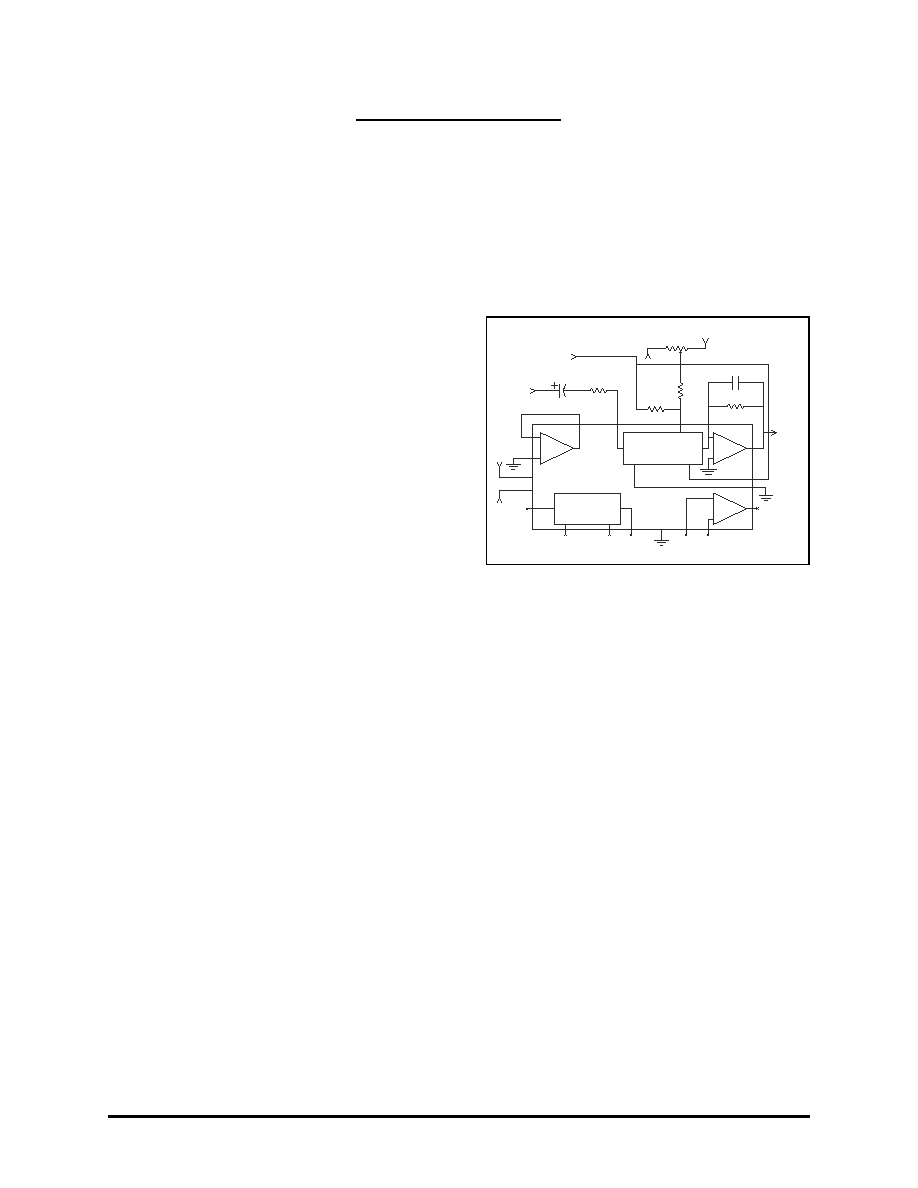
OUT
CT
IT
IN
-
+
-
1
18
11
17
14
13
12
15
16
19
20
2
5
4
9
10
8
6
7
-
OA1
+
VCC
THAT4301
EC-
EC+
IN
OUT
SYM
VCA
OA3
+
OA2
GND VEE
RMS
Fig ure 1. Block Di a gram (pin num bers are for DIP only)
Model
20 pin
DIP Pkg
30 pin DMP
(SO) Pkg
4301
RoHS
Com pli ant
4301P20-I
4301M30-I
4301A
RoHS
Com pli ant
4301AP20-I
---
4301
---
4301M30
4301A
4301AP20
---
Ta ble 1. Or der ing Information
Doc. 600069 Rev. 02

THAT Corporation; 45 Sumner Street; Milford, Massachusetts 01757-1656; USA
Tel: +1 (508) 478-9200; Fax: +1 (508) 478-0990; Web: www.thatcorp.com
Page 2
Doc u ment 600069 Rev 02
SPEC I FI CA TIONS
1,2
Ab so lute Max i mum Rat ings (T
A
= 25∞C)
Pos i tive Sup ply Volt age (V
CC
)
+18 V
Neg a tive Sup ply Volt age (V
EE
)
-18 V
Sup ply Cur rent (I
CC
)
20 mA
Power Dis si pa tion (P
D
) (T
A
= 75∞C)
700 mW
Op er ating Tem per a ture Range (T
OP
)
0 to +70∞C
Stor age Tem per a ture Range (T
ST
)
-40 to +125∞C
Over all Elec tri cal Char ac ter is tics
Pa ram e ter
Sym bol
Con di tions
Min
Typ
Max
Units
Pos i tive Sup ply Volt age
V
CC
+7
--
+15
V
Neg a tive Sup ply Volt age
V
EE
-7
--
-15
V
Pos i tive Sup ply Cur rent
I
CC
--
12
18
mA
Neg a tive Sup ply Cur rent
I
EE
--
-12
-18
mA
Ther mal Re sis tance
J-C
SO-Package
--
140
--
∞C/W
VCA Elec tri cal Char ac ter is tics
3
4301
4301A
Pa ram e ter
Sym bol
Con di tions
Min
Typ
Max
Min
Typ
Max
Units
In put Bias Cur rent
I
B(VCA)
No Sig nal
--
30
400
--
30
400
pA
In put Off set Volt age
V
OFF(VCA In)
No Sig nal
--
±
4
±
15
--
±
4
±
15
mV
In put Sig nal Cur rent
I
IN(VCA)
or I
OUT(VCA)
--
175
750
--
175
750
µ
Arms
Gain at 0V Con trol
G
0
E
C+
= E
C≠
= 0.000V
-0.4
0.0
+0.4
-0.4
0.0
+0.4
dB
Gain-Control Con stant
T
A
= 25∞C (T
CHIP
55∞C)
-60 dB < gain < +40dB
E
C+
/Gain (dB)
E
C+
& SYM
6.4
6.5
6.6
6.4
6.5
6.6
mV/dB
E
C-
/Gain (dB)
E
C-
-6.4
-6.5
-6.6
-6.4
-6.5
-6.6
mV/dB
Gain-Control TempCo
E
C
/
T
CHIP
Ref T
CHIP
= 27∞C
--
+0.33
--
--
+0.33
--
%/∞C
Gain-Control Lin ear ity
-60 to +40 dB gain
--
0.5
2
--
0.5
2
%
Off Iso la tion
E
C+
=SYM=-375mV, E
C-
=+375mV 110
115
--
110
115
--
dB
Out put Off set Volt age Change
V
OFF(OUT)
R
out
= 20k
0 dB gain
--
1
3
--
1
3
mV
+15 dB gain
--
2
10
--
2
10
mV
+30 dB gain
--
5
25
--
5
25
mV
Gain Cell Idling Cur rent
I
IDLE
--
20
--
--
20
--
µ
A
Out put Noise
e
n(OUT)
20 Hz-20 kHz
R
out
= 20k
0 dB gain
--
-96
-94
--
-96
-94
dBV
+15 dB gain
--
-85
-83
--
-85
-83
dBV
To tal Har monic Dis tor tion
THD
V
IN
= 0 dBV, 1 kHz
0 dB gain
--
0.003 0.007
--
0.003 0.007
%
1. All spec i fi ca tions sub ject to change with out no tice.
2. Unless oth er wise noted, T
A
=25∞C, V
CC
= +15V, V
EE
= -15V; VCA
SYM
ad justed for min THD @ 1 V, 1 kHz, 0 dB gain.
3. Test cir cuit is the VCA sec tion only from Fig ure 2.

THAT Corporation; 45 Sumner Street; Milford, Massachusetts 01757-1656; USA
Tel: +1 (508) 478-9200; Fax: +1 (508) 478-0990; Web: www.thatcorp.com
THAT 4301 An a log En gine IC Dy nam ics Pro ces sor
Page 3
SPEC I FI CA TIONS
1,2
(Cont'd.)
VCA Elec tri cal Char ac ter is tics
3
(Cont'd.)
4301
4301A
Pa ram e ter
Sym bol
Con di tions
Min
Typ
Max
Min
Typ
Max
Units
To tal Har monic Dis tor tion (cont'd.) THD
V
IN
= +10 dBV, 1 kHz
0 dB gain
--
0.03
0.07
--
0.03
0.07
%
≠15 dB gain
--
0.035 0.09
--
0.035 0.09
%
V
OUT
= +10 dBV, 1 kHz
+15 dB gain
--
0.035 0.09
--
0.035 0.09
%
V
IN
= +19.5 dBV, 1 kHz
0 dB gain
--
--
--
--
0.05
0.09
%
Sym me try Con trol Volt age
V
SYM
min i mum THD
-2.5
0
+2.5
-2.5
0
+2.5
mV
RMS De tec tor Elec tri cal Char ac ter is tics
4
Pa ram e ter
Sym bol
Con di tions
Min
Typ
Max
Units
In put Bias Cur rent
I
B (RMS)
No Sig nal
--
30
400
pA
In put Off set Volt age
V
OFF(RMS In)
No Sig nal
--
±
4
±
15
mV
In put Sig nal Cur rent
I
IN(RMS)
--
175
750
µ
A
In put Cur rent for 0 V Out put
I
in0
I
T
= 7.5
µ
A
6
8.5
12
µ
A
Out put Scale Fac tor
E
O
/ 20log(I
in
/I
in0
)
31.6nA< I
IN
< 1mA
T
A
= 25∞C (T
CHIP
55∞C)
6.4
6.5
6.6
mV/dB
Scale Fac tor Match (RMS to VCA)
-20 dB < VCA Gain < +20 dB
1
µ
A<I
in
(DET)
<100
µ
A
.985
1
1.015
Out put Lin ear ity
f
IN
= 1kHz
1
µ
A < I
in
< 100
µ
A
--
0.1
--
dB
100nA < I
in
< 316
µ
A
--
0.5
--
dB
31.6nA < I
in
< 1mA
--
1.5
--
dB
Rec ti fier Bal ance
f
IN
= 100 Hz,
= .001 s
1
µ
A< I
in
< 100
µ
A
≠20
--
20
%
Crest Fac tor
1ms pulse rep e ti tion rate
0.2 dB er ror
--
3.5
--
0.5 dB er ror
--
5
--
1.0 dB er ror
--
10
--
Max i mum Fre quency for 2 dB Ad di tional Er ror
I
in
10
µ
A
--
100
--
kHz
I
in
3
µ
A
--
45
--
kHz
I
in
300nA
--
7
--
kHz
Tim ing Cur rent Set Range
I
T
1.5
7.5
15
µ
A
Volt age at I
T
Pin
I
T
= 7.5
µ
A
-10
+20
+50
mV
Tim ing Cur rent Ac cu racy
I
CT
/I
T
I
T
= 7.5
µ
A
0.90
1.1
1.30
Fil tering Time Con stant
T
CHIP
= 55
∞
C
(
)
0 026
.
C
I
T
T
s
Out put Temp. Co ef fi cient
E
o
/
T
CHIP
Re: T
CHIP
= 27
∞
C
--
0.33
--
%/∞C
Out put Cur rent
I
OUT
≠300mV < V
OUT
< +300mV
±
90
±
100
--
µ
A
4. Ex cept as noted, test cir cuit is the RMS-Detector sec tion only from Fig ure 2.
THAT Corporation; 45 Sumner Street; Milford, Massachusetts 01757-1656; USA
Tel: +1 (508) 478-9200; Fax: +1 (508) 478-0990; Web: www.thatcorp.com
Page 4
Doc u ment 600069 Rev 02
Specifications
1,2
(Cont'd)
Opamp Elec tri cal Char ac ter is tics
5
OA1
OA2
OA3
Pa ram e ter
Sym bol
Con di tions
Min Typ Max
Min Typ Max
Min Typ Max
Units
In put Off set Volt age
V
OS
--
±
0.5
±
6
--
±
0.5
±
6
--
±
0.5
±
6
mV
In put Bias Cur rent
I
B
--
150 500
--
150 500
--
150 500
nA
In put Off set Cur rent
I
OS
--
15
50
--
15
50
N/A
nA
In put Volt age Range
I
VR
--
±
13.5 --
--
±
13.5 --
N/A
V
Com mon Mode Rej. Ra tio CMRR
R
S
<10k
--
100
--
--
100
--
N/A
Power Sup ply Rej. Ra tio
PSRR
VS=
±
7V to
±
15V
--
100
--
--
100
--
--
100
--
Gain Band width Prod uct
GBW
(@50kHz)
--
5
--
--
5
--
--
5
--
MHz
Open Loop Gain
A
VO
R
L
=10k
--
115
--
--
110
--
--
125
--
R
L
=2k
N/A
N/A
--
120
--
Out put Volt age Swing
V
O
@R
L
=5k
--
±
13
--
--
±
13
--
--
±
14
--
V
V
O
@R
L
=2k
N/A
N/A
--
--
±
13
--
V
Short Cir cuit Out put Cur rent
--
4
--
--
4
--
--
12
--
mA
Slew Rate
SR
--
2
--
--
2
--
--
2
--
V/
µ
s
To tal Har monic Dis tor tion
THD
1kHz, A
V
=1, R
L
=10k
-- 0.0007 0.003 -- 0.0007 0.003 -- 0.0007 0.003 %
1kHz, A
V
=≠1, R
L
= 2k
N/A
N/A
-- 0.0007 0.003 %
In put Noise Volt age Den sity
e
n
f
O
=1kHz
--
6.5
10
--
7.5
12
--
7.5
12
nV
Hz
In put Noise Cur rent Den sity
i
n
f
O
=1kHz
--
0.3
--
--
0.3
--
--
0.3
--
pA Hz
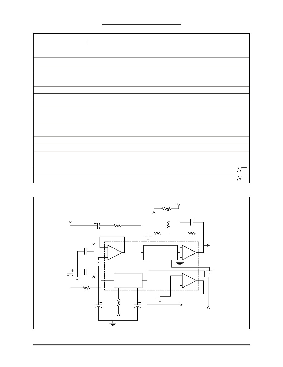
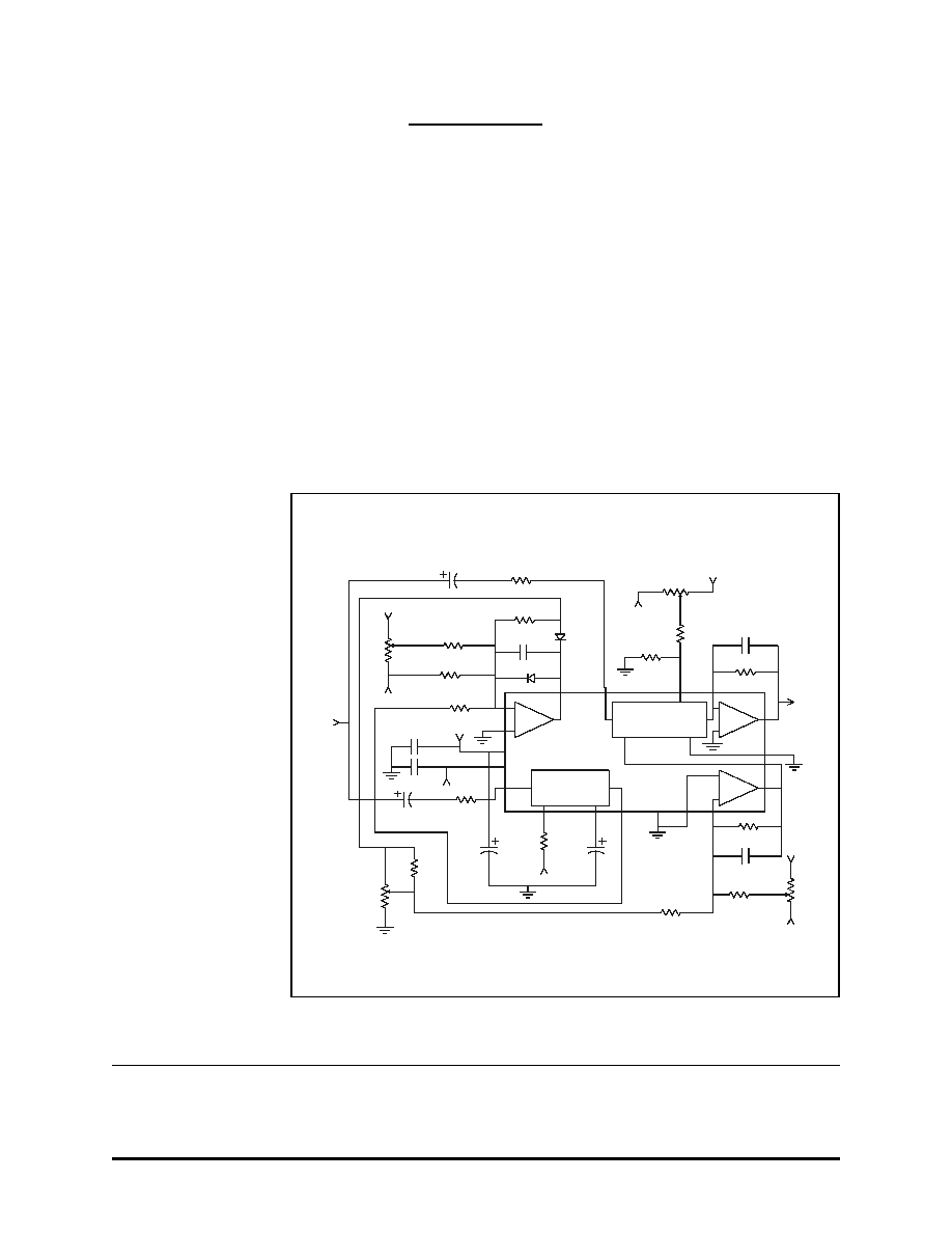
50K
R5
47uF
C1
10uF
C4
22uF
C6
300K
R4
51
R3
1%
R1
1%
R2
47pF
C2
1%
10K0
R6
47uF
C3
1%
2M00
R7
100n
C7
100n
C8
Ct
OA2
OA1
VEE
VCC
GND
-
+
VCA
-
-
+
VCA SYM
IN
SIGNAL
Ec-
OUT
SIGNAL
OUT
RMS
+15V
+15V
-15V
-15V
-15V
20K0
20K0
THAT4301
IN
RMS
It
SYM
OUT
IN
EC-
EC+
OA3
OUT
+
Fig ure 2. VCA and RMS de tec tor test cir cuit
5. Test cir cuit for opamps is a unity-gain fol lower con fig u ra tion, with load re sis tor R
L
as spec i fied.
THAT Corporation; 45 Sumner Street; Milford, Massachusetts 01757-1656; USA
Tel: +1 (508) 478-9200; Fax: +1 (508) 478-0990; Web: www.thatcorp.com
THAT 4301 An a log En gine IC Dy nam ics Pro ces sor
Page 5
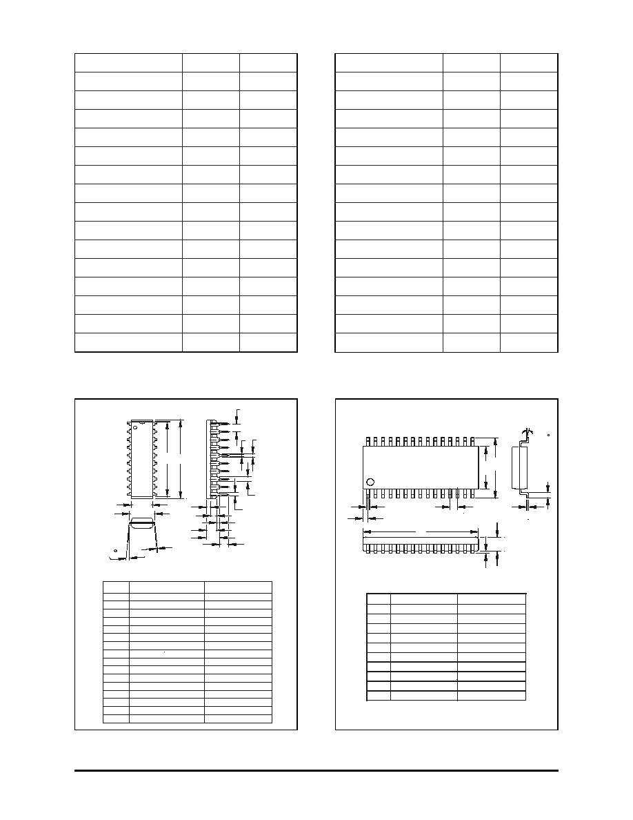
Pin Name
DIP Pin
SO Pin
RMS In
1
3
I
T
(I
Time
)
2
4
No Con nec tion
3
5
RMS Out
4
6
C
T
(C
Time
)
5
7
OA2 -In
6
9
OA2 Out
7
10
OA2 +In
8
11
GND
9
12
VEE
10
13
VCC
11
18
OA3 Out
12
19
VCA Out
13
20
SYM
14
22
E
C+
15
23
Pin Name
DIP Pin
SO Pin
E
C-
16
24
VCA In
17
25
OA1 Out
18
26
OA1 -In
19
27
OA1 +In
20
28
No Con nec tion
1
No Con nec tion
2
No Con nec tion
8
No Con nec tion
14
No Con nec tion
15
No Con nec tion
16
No Con nec tion
17
No Con nec tion
21
No Con nec tion
29
No Con nec tion
30
Ta ble 2. Pin Con nec tions
1
B
A
C
D
P
J
I
K
N
L
M
O
H
F G
E
ITEM
A
B
C
D
E
F
G
H
I
J
K
L
M
N
O
P
MILLIMETERS
INCHES
24.8 Max.
0.98 Max
24.2 +/-0.2
0.95 +/-0.008
6.4 +/-0.2
0.25 +/-0.008
7.62 +/-0.25
0.30 +/-0.01
2.54 +/-0.15
0.10 +/-0.006
0.46 +0.15 -0.1
0.02 +0.006 -0.004
1.0 +/-0.15
0.04 +/-0.006
1.5 Typ.
0.06 Typ.
0.98 Typ.
0.04 Typ.
1.5
0.06
1.75
0.07
3.25 +/-0.15
0.13 +/-0.006
4.7 Max.
0.19 Max.
0.51 Min.
0.02 Min.
2.8 Min.
0.11 Min.
0.25 +0.15 -0.05
0.01 +0.006 -0.002
0-15
Fig ure 3. Plas tic dual in-line pack age out line
B C
J
G
I
H
E
D
A
1
+ 0.1 - 0.05
Typ.
+/- 0.2
+ 0.1 - 0.05
+/- 0.4
+/- 0.3
J
0.2
I
0.8
H
0.15
G
2.3
F
0.85 MAX.
E
1.0
D
0.4
C
10.3
B
7.5
15.4
A
MILLIMETERS
ITEM
F
+/- 0.1
+/- 0.15
INCHES
0.60 +/- 0.012
0.29 +/- 0.008
0.41 +/- 0.016
0.002 +0.004 -0.002
0.039 Typ.
0.033 Max.
0.09 +/- 0.006
0.006 +/- 0.004
0.031
0.008 +0.004 -0.002
0-10
Fig ure 4. Plas tic sur face-mount pack age out line
THAT Corporation; 45 Sumner Street; Milford, Massachusetts 01757-1656; USA
Tel: +1 (508) 478-9200; Fax: +1 (508) 478-0990; Web: www.thatcorp.com
Page 6
Doc u ment 600069 Rev 02
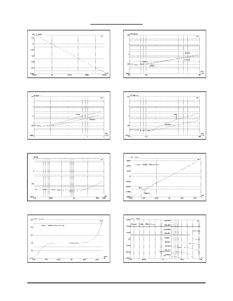
Fig ure 5. VCA Gain vs. Con trol Volt age (Ec-) at 25∞C
Fig ure 6. VCA 1kHz THD+Noise vs. In put, -15 dB Gain
Rep re sen ta tive Data
Fig ure 7. VCA 1kHz THD+Noise vs. In put, +15 dB Gain
Fig ure 8. VCA 1kHz THD+Noise vs. In put, 0 dB Gain
Fig ure 9. VCA THD vs. Fre quency, 0 dB Gain, 1Vrms Input
Fig ure 10. RMS Out put vs. In put Level, 1 kHz & 10 kHz
Fig ure 11. De par ture from Ideal De tec tor Law vs. Level
Fig ure 12. De tec tor Out put vs. Fre quency at Var i ous Levels
The ory of Op er a tion
THAT 4301 Dy nam ics Pro ces sor com bines THAT
Cor po ra tion's proven Volt age-Controlled Am pli fier
(VCA) and RMS-Level De tec tor de signs with three
gen eral-purpose opamps to pro duce an An a log En -
gine use ful in a va ri ety of dy nam ics pro ces sor ap pli -
ca tions. For de tails of the the ory of op er a tion of the
VCA and RMS-Detector build ing blocks, the in ter -
ested reader is re ferred to THAT Cor po ra tion's data
sheets on the 2150 Se ries VCAs and the 2252
RMS-Level De tec tor. The ory of the in ter con nec tion of
ex po nen tially-controlled VCAs and log-responding
level de tec tors is cov ered in THAT Cor po ra tion's ap -
pli ca tion note AN101, The Math e mat ics of
Log-Based Dy namic Pro ces sors.
The VCA -- in Brief
THAT 4301 VCA is based on THAT Cor po ra tion's
highly suc cess ful com ple men tary log-antilog gain cell
to pol ogy, as used in THAT 2150-Series IC VCAs, and
the mod u lar 202 Se ries VCAs. THAT 4301 is in te -
grated us ing a fully com ple men tary, BiFET pro cess.
The com bi na tion of FETs with high-quality, com ple -
men tary bi po lar tran sis tors (NPNs and PNPs) al lows
ad di tional flex i bil ity in the de sign of the VCA over
pre vi ous ef forts.
In put sig nals are cur rents to the VCA IN pin. This
pin is a vir tual ground, so in nor mal op er a tion an in -
put volt age is con verted to in put cur rent via an ap -
pro pri ately sized re sis tor (R
1
in Fig ure 2, Page 4).
Be cause dc off sets pres ent at the in put pin and any
dc off set in preceeding stages will be mod u lated by
gain changes (thereby be com ing au di ble as thumps),
the in put pin is nor mally ac-coupled (C
1
in Fig ure 2).
The VCA out put sig nal is also a cur rent, in verted
with re spect to the in put cur rent. In nor mal op er a -
tion, the out put cur rent is con verted to a volt age via
in verter OA
3
, where the ra tio of the con ver sion is de -
ter mined by the feed back re sis tor (R
2
, Fig ure 2) con -
nected be tween OA
3
`s out put and its in vert ing in put.
The sig nal path through the VCA and OA
3
is
noninverting.
The gain of the VCA is con trolled by the volt age
ap plied to E
C≠
, E
C+
, and SYM. Gain (in deci bels) is
pro por tional to E
C+
≠ E
C-
, pro vided E
C+
and SYM are
at es sen tially the same volt age (see be low). The con -
stant of pro por tion al ity is ≠6.5 mV/dB for the volt age
at E
C≠
, and 6.5 mV/dB for the volt age at E
C+
and SYM.
As men tioned, for proper op er a tion, the same
volt age must be ap plied to E
C+
and SYM, ex cept for a
small (
±
2.5 mV) dc bias ap plied be tween these pins.
This bias volt age ad justs for in ter nal mis matches in
the VCA gain cell which would oth er wise cause small
dif fer ences be tween the gain of pos i tive and neg a tive
half-cycles of the sig nal. The volt age is usu ally ap -
plied via an ex ter nal trim po ten ti om e ter (R
5
in Fig ure
2), which is ad justed for min i mum sig nal dis tor tion
at unity (0 dB) gain.
The VCA may be con trolled via E
C-
, as shown in
Fig ure 2, or via the com bi na tion of E
C+
and SYM.
This con nec tion is il lus trated in Fig ure 13. Note that
this fig ure shows only that por tion of the cir cuitry
needed to drive the pos i tive VCA con trol port; cir -
cuitry as so ci ated with OA
1
, OA
2
and the RMS de tec tor
has been omit ted.
While the 4301's VCA cir cuitry is very sim i lar to
that of the THAT 2150 Se ries VCAs, there are sev eral
im por tant dif fer ences, as fol lows:
1) Sup ply cur rent for the VCA is fixed in ter nally.
Ap prox i mately 2mA is avail able for the sum of in put
and out put sig nal cur rents. (This is also the case in a
2150 Se ries VCA when bi ased as rec om mended.)
2) The sig nal cur rent out put of the VCA is in ter -
nally con nected to the in vert ing in put of an on-chip
opamp. In or der to pro vide ex ter nal feed back around
this opamp, this node is brought out to a pin.
3) The con trol-voltage con stant is ap prox i mately
6.5 mV/dB, due pri mar ily to the higher in ter nal op er -
at ing tem per a ture of the 4301 com pared to that of
the 2150 Se ries.
4) The in put stage of the 4301 VCA uses in te -
grated P-channel FETs rather than a bias-current
cor rected bi po lar dif fer en tial am pli fier. In put bias
cur rents have there fore been re duced.
The RMS De tec tor -- in Brief
The 4301's de tec tor com putes rms level by rec ti -
fy ing in put cur rent sig nals, con vert ing the rec ti fied
cur rent to a log a rith mic volt age, and ap ply ing that
volt age to a log-domain fil ter. The out put sig nal is a
dc volt age pro por tional to the deci bel-level of the rms
THAT Corporation; 45 Sumner Street; Milford, Massachusetts 01757-1656; USA
Tel: +1 (508) 478-9200; Fax: +1 (508) 478-0990; Web: www.thatcorp.com
THAT 4301 An a log En gine IC Dy nam ics Pro ces sor
Page 7
50K
R5
47uF
C1
300K
R4
51
R3
1%
20K0
R1
1%
20K0
R2
47pF
C2
Ct
It
THAT4301
OUT
SYM
OUT
OA3
OA2
OA1
VEE
VCC
GND
IN
RMS
-
+
EC+
EC-
IN
VCA
-
-
+
+
VCA SYM
Signal In
Positive Control In
Signal
Out
Fig ure 13. Driving the VCA via the Pos i tive Con trol Port

value of the in put sig nal cur rent. Some ac com po nent
(at twice the in put fre quency) re mains su per im posed
on the dc out put. The ac sig nal is at ten u ated by a
log-domain fil ter, which con sti tutes a sin gle-pole
rolloff with cut off de ter mined by an ex ter nal ca pac i -
tor and a pro gram ma ble dc cur rent.
As in the VCA, in put sig nals are cur rents to the
RMS IN pin. This in put is a vir tual ground, so a re -
sis tor (R
6
in Fig ure 2) is nor mally used to con vert in -
put volt ages to the de sired cur rent. The level de tec tor
is ca pa ble of ac cu rately re solv ing sig nals well be low
10 mV (with a 10 k
in put re sis tor). How ever, if the
de tec tor is to ac cu rately track such low-level sig nals,
ac cou pling is nor mally re quired.
The log-domain fil ter cut off fre quency is usu ally
placed well be low the fre quency range of in ter est. For
an au dio-band de tec tor, a typ i cal value would be
5 Hz, or a 32 ms time con stant (
). The fil ter's time
con stant is de ter mined by an ex ter nal ca pac i tor at -
tached to the C
T
pin, and an in ter nal cur rent source
(I
CT
) con nected to C
T
. The cur rent source is pro -
grammed via the I
T
pin: cur rent in I
T
is mir rored to
I
CT
with a gain of ap prox i mately 1.1. The re sult ing
time con stant
is ap prox i mately equal to 0.026 C
T
/I
T
.
Note that, as a re sult of the math e mat ics of RMS de -
tec tion, the at tack and re lease time con stants are
fixed in their re la tion ship to each other.
The dc out put of the de tec tor is scaled with the
same con stant of pro por tion al ity as the VCA gain
con trol: 6.5 mV/dB. The de tec tor's 0 dB ref er ence
(I
in0
, the in put cur rent which causes 0 V out put), is
de ter mined by I
T
as fol lows: I
in0
= 9.6 mA I
t
The de -
tec tor out put stage is ca pa ble of sink ing or sour cing
100
µ
A.
Dif fer ences be tween the 4301's RMS-Level De tec -
tor cir cuitry and that of the THAT 2252 RMS De tec -
tor are as fol lows:
1) The rec ti fier in the 4301 RMS De tec tor is in ter -
nally bal anced by de sign, and can not be bal anced
via an ex ter nal con trol. The 4301 will typ i cally bal -
ance pos i tive and neg a tive halves of the in put sig nal
within
±
1.5%, but in ex treme cases the mis match
may reach
±
15%. How ever, a 15% mis match will
not sig nif i cantly in crease rip ple-induced dis tor tion
in dy nam ics pro ces sors over that caused by sig nal
rip ple alone.
2) The time con stant of the 4301's RMS de tec tor is
de ter mined by the com bi na tion of an ex ter nal ca -
pac i tor (con nected to the C
T
pin) and an in ter nal,
pro gram ma ble cur rent source. The cur rent source
is equal to 1.1 I
T
. Normally, a re sis tor is not con -
nected di rectly to the C
T
pin on the 4301.
3) The 0 dB ref er ence point, or level match, is not
ad just able via an ex ter nal cur rent source. How ever,
as in the 2252, the level match is af fected by the
tim ing cur rent, which, in this case, is drawn from
the I
T
pin and mir rored in ter nally to C
T
.
4) The in put stage of the 4301 RMS de tec tor uses
in te grated P-channel FETs rather than a
bias-current cor rected bi po lar dif fer en tial am pli fier.
In put bias cur rents are there fore neg li gi ble, im prov -
ing per for mance at low sig nal lev els.
The Opamps -- in Brief
The three opamps in the 4301 are in tended for
gen eral pur pose ap pli ca tions. All are 5 MHz opamps
with slew rates of ap prox i mately 2V/
µ
s. All use bi po -
lar PNP in put stages. How ever, the de sign of each is
op ti mized for its ex pected use. There fore, to get the
most out of the 4301, it is use ful to know the ma jor
dif fer ences among these opamps.
OA
3
, be ing in ter nally con nected to the out put of
the VCA, is in tended for cur rent-to-voltage con ver -
sion. Its in put noise per for mance, at 7 5
.
nV
Hz, com
-
ple ments that of the VCA, add ing neg li gi ble noise at
unity gain. Its out put sec tion is ca pa ble of driv ing a
2 k
load to within 2V of the power sup ply rails,
mak ing it pos si ble to use this opamp di rectly as the
out put stage in sin gle-ended de signs.
OA
1
is the qui et est opamp of the three. Its in put
noise volt age, at 6 5
.
nV
Hz, makes it the opamp of
choice for in put stages. Note that its out put drive ca -
pa bil ity is lim ited (in or der to re duce the chip's
power dis si pa tion) to ap prox i mately
±
3 mA. It is
com fort able driv ing loads of 5 k
or more to within
1V of the power sup ply rails.
OA
2
is in tended pri mar ily as a con trol-voltage
pro ces sor. Its in put noise par al lels that of OA
3
, and
its out put drive ca pa bil ity par al lels that of OA
1
.
THAT Corporation; 45 Sumner Street; Milford, Massachusetts 01757-1656; USA
Tel: +1 (508) 478-9200; Fax: +1 (508) 478-0990; Web: www.thatcorp.com
Page 8
Doc u ment 600069 Rev 02
Ap pli ca tions
The cir cuit of Fig ure 14, Page 9, shows a typ i cal
ap pli ca tion for THAT 4301. This sim ple com pres -
sor/lim iter de sign fea tures ad just able hard-knee
thresh old, com pres sion ra tio, and static gain
1
. The
ap pli ca tions dis cus sion in this data sheet will cen ter
on this cir cuit for the pur pose of il lus trat ing im por -
tant de sign is sues. How ever, it is posslble to con fig -
ure many other types of dy nam ics pro ces sors with
THAT 4301. Hope fully, the fol low ing dis cus sion will
im ply some of these pos si bil i ties.
Sig nal Path
As men tioned in the sec tion on the ory, the VCA
in put pin is a vir tual ground with neg a tive feed back
pro vided in ter nally. An in put re sis tor (R
1
, 20k
) is
re quired to con vert the ac in put volt age to a cur rent
within the lin ear range of the 4301. (Peak VCA in put
cur rents should be kept un der 1 mA for best dis tor -
tion per for mance.) The cou pling ca pac i tor (C
1
, 47
µ
f)
is strongly rec om -
mended to block dc cur -
rent from preceeding
stages (and from off set
volt age at the in put of
the VCA). Any dc cur rent
into the VCA will be
mod u lated by vary ing
gain in the VCA, show ing
up in the out put as
"thumps". Note that C
1
,
in con junc tion with R
1
,
will set the low fre -
quency limit of the cir -
cuit.
The VCA out put is
con nected to OA
3
, con fig -
ured as an in vert ing cur -
rent-to-voltage con verter.
OA
3
`s feed back com po -
nents (R
2
, 20 k
, and
C
2
, 47 pf) de ter mine the
con stant of cur -
rent-to-voltage con ver -
sion. The sim plest way
to deal with this is to
rec og nize that when the
VCA is set for unity
(0 dB) gain, the in put to
out put volt age gain is
sim ply R
2
/R
1
, just as in
the case of a sin gle in -
vert ing stage. If, for some rea son, more than 0 dB
gain is re quired when the VCA is set to unity, then
the re sis tors may be skewed to pro vide it. Note that
the feed back ca pac i tor (C
2
) is re quired for sta bil ity.
The VCA out put has ap prox i mately 45 pf of ca pac i -
tance to ground, which must be neu tral ized via the
47 pf feed back ca pac i tor across R
2
.
The VCA gain is con trolled via the E
C≠
ter mi nal,
whereby gain will be pro por tional to the neg a tive of
the volt age at E
C≠
. The E
C+
ter mi nal is grounded, and
the SYM ter mi nal is re turned nearly to ground via a
small re sis tor (R
3
, 51
). The VCA SYM trim (R
5
,
50 k
) al lows a small volt age to be ap plied to the
SYM ter mi nal via R
4
(300 k
). This volt age ad justs
for small mis matches within the VCA gain cell,
thereby re duc ing even-order dis tor tion prod ucts. To
ad just the trim, ap ply to the in put a mid dle-level,
mid dle-frequency sig nal (1 kHz at 1 V is a good
THAT Corporation; 45 Sumner Street; Milford, Massachusetts 01757-1656; USA
Tel: +1 (508) 478-9200; Fax: +1 (508) 478-0990; Web: www.thatcorp.com
THAT 4301 An a log En gine IC Dy nam ics Pro ces sor
Page 9
CR2
10K0
R9
22p
C9
1%
EC+
EC-
IN
OUT
SYM
VCA
+
OA3
-
OUT
1%
20K0
R2
51
R3
R16
1%
4k99
+
OA2
-
GND
C5
100N
1%
590K
R17
1%
10K0
R15
+15
R18
CCW
CW
GAIN
10K
-15
1%
1K43
R14
COMPRESSION
CW
CCW
R13
10K
C3
47uF
R6
-15
10K0 1%
22uF
C6
IN
IT
OUT
CT
RMS
R7
2M00
1%
-15
10uF
C4
VEE
VCC
THAT4301
+15
100n
C7
C8 100n
1%
4k99
R8
+
OA1
-
-15
2M00 1%
R10
1%
383K
R11
CR1
R12
CW
10K
CCW
THRESHOLD
+15
20K0 1%
R1
47uF
C1
300K
R4
-15
+15
R5
50K
VCA SYM
C2
47pF
IN
Fig ure 14. Typ i cal Com pres sor/Lim iter Ap pli ca tion Cir cuit
1. More in for ma tion on this com pres sor de sign, along with sug ges tions for con vert ing it to soft-knee op er a tion,
is given in AN100, Ba sic Com pres sor Lim iter De sign. The de signs in AN100 are based on THAT Cor po ra tion's
2150-Series VCAs and 2252 RMS De tec tor, but are readily adapt able to the 4301 with only mi nor mod i fi ca tions. In
fact, the cir cuit pre sented here is func tion ally iden ti cal to the hard-knee cir cuit pub lished in AN100.

choice with this cir cuit) and ob serve THD at the sig -
nal out put. Set the trim for min i mum THD.
RMS-Level De tec tor
The RMS de tec tor's in put is sim i lar to that of the
VCA. An in put re sis tor (R
6
, 10 k
) con verts the ac in -
put volt age to a cur rent within the lin ear range of the
4301. (Peak de tec tor in put cur rents should be kept
un der 1 mA for best lin ear ity.) The cou pling ca pac i tor
(C
3
, 47
µ
f) is rec om mended to block dc cur rent from
preceeding stages (and from off set volt age at the in -
put of the de tec tor). Any dc cur rent into the de tec tor
will limit the low-level res o lu tion of the de tec tor, and
will up set the rec ti fier bal ance at low lev els. Note
that, as with the VCA in put cir cuitry, C
3
in con junc -
tion with R
6
will set the lower fre quency limit of the
de tec tor.
The time re sponse of the RMS de tec tor is de ter -
mined by the ca pac i tor at tached to C
T
(C
4
, 10
µ
f) and
the size of the cur rent in pin I
T
(de ter mined by R
7
,
2 M
and the neg a tive power sup ply, ≠15V). Since the
volt age at I
T
is ap prox i mately 0 V, the cir cuit of Fig ure
14 pro duces 7.5
µ
A in I
T
. The cur rent in I
T
is mir -
rored with a gain of 1.1 to the C
T
pin, where it is
avail able to dis charge the tim ing ca pac i tor (C
4
). The
com bi na tion pro duces a log fil ter with time con stant
equal to ap prox i mately 0.026 C
T
/I
T
(~35 ms in the
cir cuit shown).
The wave form at C
T
will fol low the logged (deci -
bel) value of the in put sig nal en ve lope, plus a dc off -
set of about 1.3 V (2 V
BE
). This al lows a po lar ized
ca pac i tor to be used for the tim ing ca pac i tor, usu ally
an elec tro lytic. The ca pac i tor used should be a
low-leakage type in or der not to add sig nif i cantly to
the tim ing cur rent.
The out put stage of the RMS de tec tor serves to
buffer the volt age at C
T
and re move the 1.3 V dc off -
set, re sult ing in an out put cen tered around 0 V for in -
put sig nals of about 85 mV. The out put volt age
in creases 6.5 mV for ev ery 1 dB in crease in in put sig -
nal level. This re la tion ship holds over more than a
60 dB range in in put cur rents.
Con trol Path
A com pres sor/lim iter is in tended to re duce its
gain as sig nals rise above a thresh old. The out put of
the RMS de tec tor rep re sents the in put sig nal level
over a wide range of lev els, but com pres sion only oc -
curs when the level is above the thresh old. OA
1
is
con fig ured as a vari able thresh old de tec tor to block
en ve lope in for ma tion for low-level sig nals, pass ing
only in for ma tion for sig nals above thresh old.
OA
1
is an in vert ing stage with gain of 2 above
thresh old and 0 be low thresh old. Ne glecting the ac -
tion of the THRESH OLD con trol (R
12
) and its as so ci -
ated re sis tors (R
11
and R
10
), pos i tive sig nals from the
RMS de tec tor out put drive the out put of OA
1
neg a -
tive. This for ward bi ases CR
2
, clos ing the feed back
loop such that the junc tion of R
9
and CR
2
(the out put
of the thresh old de tec tor) sits at -(R
9
/R
8
) RMS
OUT
. For
the cir cuit of Fig ure 14, this is ≠2 RMS
OUT
. Neg a tive
sig nals from the RMS de tec tor drive the out put of
OA
1
pos i tive, re verse bi as ing CR
2
and for ward bi as ing
CR
1
. In this case, the junc tion of R
9
and CR
2
rests at
0 V, and no sig nal level informaion is passed to the
thresh old de tec tor's out put.
In or der to vary the thresh old, R
12
, the THRESH -
OLD con trol, is pro vided. Via R
11
(383 k
), R
12
adds
up to
±
39.2
µ
A of cur rent to OA
1
`s sum ming junc tion,
re quir ing the same amount of op po site-polarity cur -
rent from the RMS de tec tor out put to coun ter bal ance
it. At 4.99 k
, the volt age across R
8
re quired to pro -
duce a coun ter bal anc ing cur rent is
±
195 mV, which
rep re sents a
±
30 dB change in RMS de tec tor in put
level.
Since the RMS de tec tor's 0 dB ref er ence level is
85 mV, the cen ter of the THRESH OLD pot's range
would be 85 mV, were it not for R
10
(2 M
), which
pro vides an off set. R
10
adds an ex tra ≠7.5
µ
a to OA
1
`s
sum ming junc tion, which would be coun ter bal anced
by 37.4 mV at the de tec tor out put. This cor re sponds
to 5.8 dB, off set ting the THRESH OLD cen ter by this
much to 165 mV, or ap prox i mately -16 dBV.
The out put of the thresh old de tec tor rep re sents
the sig nal level above the de ter mined thresh old, at a
con stant of about 13 mV/dB (from
[R
9
/R
8
] 6.5 mV/dB). This sig nal is passed on to the
COM PRES SION con trol (R
13
), which vari ably at tenu -
ates the sig nal passed on to OA
2
. Note that the gain of
OA
2
, from the wiper of the COM PRES SION con trol to
OA
2
`s out put, is R
16
/R
15
(0.5), pre cisely the in verse of
the gain of OA
1
. There fore, the COM PRES SION con -
trol lets the user vary the above-threshold gain be -
tween the RMS de tec tor out put and the out put of OA
1
from zero to a max i mum of unity.
The gain con trol con stant of the VCA, 6.5 mV/dB,
is ex actly equal to the out put scal ing con stant of the
RMS de tec tor. There fore, at max i mum COM PRES -
SION, above thresh old, ev ery dB in crease in in put
sig nal level causes a 6.5 mV in crease in the out put of
OA
2
, which in turn causes a 1 dB de crease in the VCA
gain. With this set ting, the out put will not in crease
de spite large in creases in in put level above thresh old.
This is in fi nite com pres sion. For in ter me di ate set -
tings of COM PRES SION, a 1 dB in crease in in put sig -
nal level will cause less than a 1 dB de crease in gain,
thereby vary ing the com pres sion ra tio.
The re sis tor R
14
is in cluded to al ter the taper of
the COM PRES SION pot to better suit com mon use. If
a lin ear taper pot is used for R
13
, the com pres sion ra -
tio will be 1:2 at the mid dle of the ro ta tion. How ever,
1:2 com pres sion in an above-threshold com pres sor
is not very strong pro cess ing, so 1:4 is of ten pre -
ferred at the mid point. R
14
warps the taper of R
13
so
that 1:4 com pres sion oc curs at ap prox i mately the
mid point of R
13
`s ro ta tion.
THAT Corporation; 45 Sumner Street; Milford, Massachusetts 01757-1656; USA
Tel: +1 (508) 478-9200; Fax: +1 (508) 478-0990; Web: www.thatcorp.com
Page 10
Doc u ment 600069 Rev 02

The GAIN con trol (R
18
) is used to pro vide static
gain or at ten u a tion in the sig nal path. This con trol
adds up to
±
130 mV off set to the out put of OA
2
(from
-V
+
R
R
16
17
to -V
-
R
R
16
17
), which is ap prox i mately
±
20 dB change in gain of the VCA. C
5
is used to at ten -
u ate the noise of OA
2
, OA
1
and the re sis tors R
8
through R
16
used in the con trol path. All these ac tive
and pas sive com po nents pro duce noise which is
passed on to the con trol port of the VCA, caus ing
mod u la tion of the sig nal. By it self, the 4301 VCA pro -
duces very lit tle noise mod u la tion, and its per for -
mance can be sig nif i cantly de graded by the use of
noisy com po nents in the con trol volt age path.
Over all Re sult
The re sult ing com pres sor cir cuit pro vides
hard-knee com pres sion above thresh old with three
es sen tial user-adjustable con trols. The thresh old of
com pres sion may be var ied over a
±
30 dB range from
about ≠46 dBV to +14 dBV. The com pres sion ra tio
may be var ied from 1:1 (no com pres sion) to
:1.
And, static gain may be added up to
±
20 dB. Au dio
per for mance is ex cel lent, with THD run ning be low
0.05% at mid dle fre quen cies even with 10 dB of com -
pres sion, and an in put dy namic range of over
115 dB.
Per haps most im por tant, this ex am ple de sign
only scratches the sur face of the large body of ap pli -
ca tions cir cuits which may be con structed with THAT
4301. The com bi na tion of an ac cu rate,
wide-dynamic-range, log-responding level de tec tor
with a high-quality, ex po nen tially-responding VCA
pro duces a ver sa tile and pow er ful an a log en gine. The
opamps pro vided in the 4301 en able the de signer to
con fig ure these build ing blocks with few ex ter nal
com po nents to con struct gates, ex pand ers, de-essers,
noise re duc tion sys tems and the like.
For fur ther in for ma tion, sam ples and pric ing,
please con tact us at the ad dress be low.
THAT Corporation; 45 Sumner Street; Milford, Massachusetts 01757-1656; USA
Tel: +1 (508) 478-9200; Fax: +1 (508) 478-0990; Web: www.thatcorp.com
THAT 4301 An a log En gine IC Dy nam ics Pro ces sor
Page 11

Notes
THAT Corporation; 45 Sumner Street; Milford, Massachusetts 01757-1656; USA
Tel: +1 (508) 478-9200; Fax: +1 (508) 478-0990; Web: www.thatcorp.com
Page 12
Doc u ment 600069 Rev 02